The de Broglie hypothesis, formulated in 1924, predicts that particles should also behave as waves. De Broglie's formula was confirmed three years later for electrons (which have a rest-mass) with the observation of electron diffraction in two independent experiments. At the University of Aberdeen George Paget Thomson passed a beam of electrons through a thin metal film and observed the predicted interference patterns. At Bell Labs Clinton Joseph Davisson and Lester Halbert Germer guided their beam through a crystalline grid. Thomson and Davisson shared the Nobel Prize for Physics in 1937 for their work.
Electron interaction with matter[edit]
Unlike other types of radiation used in diffraction studies of materials, such as X-rays and neutrons, electrons are charged particles and interact with matter through the Coulomb forces. This means that the incident electrons feel the influence of both the positively charged atomic nuclei and the surrounding electrons. In comparison, X-rays interact with the spatial distribution of the valence electrons, while neutrons are scattered by the atomic nuclei through the strong nuclear forces. In addition, the magnetic moment of neutrons is non-zero, and they are therefore also scattered by magnetic fields. Because of these different forms of interaction, the three types of radiation are suitable for different studies.
Intensity of diffracted beams[edit]
In the kinematical approximation for electron diffraction, the intensity of a diffracted beam is given by:
Here is the wavefunction of the diffracted beam and is the so-called structure factor which is given by:
where is the scattering vector of the diffracted beam, is the position of an atom in the unit cell, and is the scattering power of the atom, also called the atomic form factor. The sum is over all atoms in the unit cell.
The structure factor describes the way in which an incident beam of electrons is scattered by the atoms of a crystal unit cell, taking into account the different scattering power of the elements through the factor . Since the atoms are spatially distributed in the unit cell, there will be a difference in phase when considering the scattered amplitude from two atoms. This phase shift is taken into account by the exponential term in the equation.
The atomic form factor, or scattering power, of an element depends on the type of radiation considered. Because electrons interact with matter though different processes than for example X-rays, the atomic form factors for the two cases are not the same.
Wavelength of electrons[edit]
Here is Planck's constant and the relativistic momentum of the electron. is called the de Broglie wavelength. The electrons are accelerated in an electric potential to the desired velocity:
is the mass of the electron, and is the elementary charge.The electron wavelength is then given by:
However, in an electron microscope, the accelerating potential is usually several thousand volts causing the electron to travel at an appreciable fraction of the speed of light. A SEM may typically operate at an accelerating potential of 10, 000 volts (10 kV) giving an electron velocity approximately 20% of the speed of light, while a typical TEM can operate at 200 kV raising the electron velocity to 70% the speed of light. We therefore need to take relativistic effects into account. The relativistic relation between energy and momentum is E2=p2c2+m02c4 and it can be shown that,
where ΔE = E − E0 = eU. The relativistic formula for the wavelength is then modified to become,
is the speed of light. We recognize the first term in this final expression as the non-relativistic expression derived above, while the last term is a relativistic correction factor. The wavelength of the electrons in a 10 kV SEM is then 12.2 x 10⁻¹² m (12.2 pm) while in a 200 kV TEM the wavelength is 2.5 pm. In comparison the wavelength of X-rays usually used in X-ray diffraction is in the order of 100 pm (Cu Kα: λ=154 pm).
Electron diffraction in a TEM[edit]
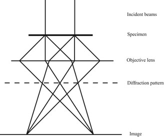
Electron diffraction of solids is usually performed in a Transmission Electron Microscope (TEM) where the electrons pass through a thin film of the material to be studied. The resulting diffraction pattern is then observed on a fluorescent screen, recorded on photographic film, on imaging plates or using a CCD camera.
Benefits[edit]
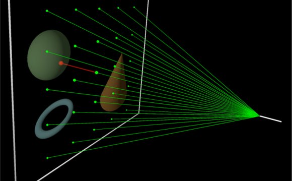
Wide angle view of TEM diffraction tilting.
As mentioned above, the wavelength of an electron accelerated in a TEM is much smaller than that of the radiation usually used for X-ray diffraction experiments. A consequence of this is that the radius of the Ewald sphere is much larger in electron diffraction experiments than in X-ray diffraction. This allows the diffraction experiment to reveal more of the two-dimensional distribution of reciprocal lattice points.
Furthermore, electron lenses allows the geometry of the diffraction experiment to be varied. The conceptually simplest geometry referred to as selected area electron diffraction (SAED) is that of a parallel beam of electrons incident on the specimen, with the specimen field selected using a sub-specimen image-plane aperture. However, by converging the electrons in a cone onto the specimen, one can in effect perform a diffraction experiment over several incident angles simultaneously. This technique is called Convergent Beam Electron Diffraction (CBED) and can reveal the full three-dimensional symmetry of the crystal.
In a TEM, a single crystal grain or particle may be selected for the diffraction experiments. This means that the diffraction experiments can be performed on single crystals of nanometer size, whereas other diffraction techniques would be limited to studying the diffraction from a multicrystalline or powder sample. Furthermore, electron diffraction in TEM can be combined with direct imaging of the sample, including high resolution imaging of the crystal lattice, and a range of other techniques. These include solving and refining crystal structures by electron crystallography, chemical analysis of the sample composition through energy-dispersive X-ray spectroscopy, investigations of electronic structure and bonding through electron energy loss spectroscopy, and studies of the mean inner potential through electron holography.
Practical aspects[edit]
1: Sketch of the electron beam-path in a TEM. 2: Typical electron diffraction pattern obtained in a TEM with a parallel electron beam
creation festival past lineups creation x design studio creativity vs logic creative form drawing pdf creation salon near me creative expressions creative under bed storage creation club fallout 4 creative under the sea costume idea creativity to solve a problem creativity by design creativity under the gun at litmus corporation slideshare creation nails and spa creation hymn creativity after retirement before creation you knew my name lyrics creative off synonym creativity after drinking alcohol creation proclaims the glory of god creativity pro creativity without boundaries creation verses creatives glassdoor creativity around globe creativity in psychology what is the difference between creativity and imagination creative at home date ideas creative kidstuff creativity to be acquired in education itself creation about definition byta från creative till survival creation antonyms creative after school program creativity journal creation tattoo creation from nothing creativity as a value delay thread creation until needed creativity through education creation x570 creative drive thru greetings creation god creation youth lesson creativity questions creativity and structure creative hobbies creativity over zoom opposite of creative subjects creative backsplash behind stove creation vs destruction asset creation under mgnrega creation usa creativity before consumption creativity xl kipling creativity justified creativity on tiktok creation science definition creativity by julia creative off creative at home creation before genesis creative through collaborationRELATED VIDEO

RELATED FACTS
-
Electron diffraction refers to the wave nature of electrons. However, from a technical or practical point of view, it may be regarded as a technique used to study matter by firing electrons at a sample and observing the resulting interference pattern. This...
-
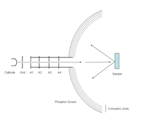
Low-energy electron diffraction (LEED) is a technique for the determination of the surface structure of crystalline materials by bombardment with a collimated beam of low energy electrons (20-200eV) and observation of diffracted electrons as spots on a fluorescent...
-
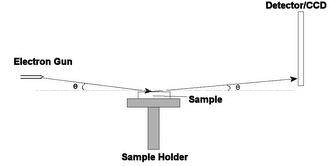
Reflection high-energy electron diffraction (RHEED) is a technique used to characterize the surface of crystalline materials. RHEED systems gather information only from the surface layer of the sample, which distinguishes RHEED from other materials characterization...
Share this Post
latest post
-
 New hologram April 27, 2026
 -
 Hologram real April 17, 2026
 -
 Wikia hologram April 7, 2026
 -
 Hologram theory March 28, 2026
 -
 Future Holograms March 18, 2026
 -
 What is diffraction? March 8, 2026
 -
 Print Holograms February 26, 2026
 -
 Holographic Future February 16, 2026